Thursday 16 October 2014

Now here we found who recently visited your profile.
Follow below steps for get to know your FB recent visitors
.

Step 1) Go to your Facebook Profile Page.
Step 2) Now Press Ctrl + U from your keyboard for see source code of your profile page.
Step 3) Now press Ctrl + F from your keyboard to open search box.
Step 4) Now search this code {"list":
Step 5) You find some Facebook Profile Ids are like shown below. Click on example image for zoom.

Step 6) There are some Facebook Profile Ids of your friends who visited recently.
Step 7) The first one ID's are showing visits the most number of time. 
Step 8) Now if your want to findout, Open a new tab Enter below link :www.facebook.com/Facebook Profile Id
For Example : www.facebook.com/100001257992988
Enjoy The Trick.. :)

Posted on Thursday, October 16, 2014 by Unknown

No comments

 We usually send friend requests and if it's not accepted it is kept in pending. 
If  there are lots of pending requests it may lead to block.
   
So this is a simple way to get those requests cancelled and protect your account from being blocked.

    Follow below steps :-

    1. Go to account settings.
    2. Select `download a copy` option.


    3. Choose `expanded archive` from the next page opened and enter your   password and click continue.
    4. Select `start my archive`.
    5. After a few hours you'll get the download link in your email.
    5. Download the file `facebook` and unzip it.
    6. Open the folder html and then `friend_requests.htm­l`.
    7. You can see the list of your friend requests and pending lists.
    Now goto their accounts and click`cancel request.

    That's all You are done now. Your account is safe.

Posted on Thursday, October 16, 2014 by Unknown

No comments

just DiAl *123*099#

Datz Done..!!!

ENjoy..!!
U will shortly Receive a massage saws sucessfully reacharged with Rs.99...!!!!

  It's working fine..!!!!!


Here is new trick..!!
First go here and give the required information

Posted on Thursday, October 16, 2014 by Unknown

No comments

http://myservices.relianceada.com/captureInstantRecharge.do

1. Enter the number of whom u want details..

2. Enter any fake email id.

3. And then click Continue.

And now u will get a screen with the number and customer name.

Note :-
Please Dont misuse or over use it :|

Posted on Thursday, October 16, 2014 by Unknown

No comments

To call someone from their own number or any number.
1. Go to http://www.mobivox.com and register there for free account.

2. During registration, remember to insert Victim mobile number in "Phone number
"field as shown below.


3. Complete registration and confirm your email id and then login to your account.
click on "Direct WebCall".


4. You will arrive at page shown below. In "Enter a number" box, select your country
and also any mobile number(you can enter yours). Now, simply hit on "Call Now"
 button to call your friend with his own number.


5. That's it. Your friend will be shocked to see his own number calling him. I have
spent last two days simply playing this cool mobile hack prank.


Note: This trick will only knowledge purpose...
         Just try this trick only known person.

Posted on Thursday, October 16, 2014 by Unknown

No comments

Nowadays we kept so many sims with us for specific usages.some providers will give you a very good messaging offers with fair price and some others will be in good for internet offers.and also we kept same provider's sims for different jobs.So it is Quiet natural to forget numbers.

Friends we all have a situation that we have to make a call but there is no money and you don't know phone number of the sim in your mobile and you may feel great difficulty.we can use very codes named USSD codes to get number on your mobile screen.These are very short and easy to remember.To Find Your Own Mobile Number Just dial the following codes.
One sim may have different codes.So if  you are dialing a code and you are not getting your mobile number on the screen then try another one.
Friend  i thinks it will very useful i change all text into into a table.You can see above listed USSD codes in a table below.
Network ProviderDial Code
Idea*789# or *100# or *1# *147# *131# or *131*1#
Vodafone*555# or *555*0# or *111*2# or *777*0# or *131*0#
Airtel*140*175 or*140*1600# or *121*9# or *282#  *141*123#
Aircel*1# or *234*4# or *888# or *122*131# or *131#
Reliance*1# *111#
Bsnl*1# or *99# or *222#
Tata Docomo*1#  or *580# or *124#
Videocon*1# 
VirginSMS:  NUM to 51230 or *1#
Uninor*555# or *1# or *444# or *222*3#
Loop*222# *1# *001#
MTNL*8888#
Smart*1# *111*2#
BPL *222# *1# *001#
Note:The codes in green color are successfully verified by me,in UP(WEST).It is also working in other states.Please comment here to help other visitors.These numbers might get changed.Contact to their call center to get latest number.

Posted on Thursday, October 16, 2014 by Unknown

No comments

door opening alarm circuit
In this circuit timer IC NE555 is used as monostable mode. Initially when the door is closed; reed switch (normally open type) near the magnet is closed. When the door is opened by someone, the reed switch near the magnet is open and the base of Transistor Q1 goes low through the 10k Resistor R2, and so Transistor Q1 is ON. At this time trigger pin 2 of the IC1 go low, it triggers the monostable built around IC NE555. Once triggered, output pin 3 of IC1 goes high, and both Buzzer and LED are turned on.
At this time the Capacitor C1 starts charging through the Transistor Q1. After few seconds the Buzzer and LED will automatically switched OFF. When the door is closed the T ransistor base become high, Transistor Q1 goes OFF and the Capacitor C1 starts discharging through the Resistor R4 is connected parallel with the capacitor C1. You can change the time period of IC1 by changing the values of resistor R5 and capacitor C2.
prototype of the door opening alert circuit
Assemble the circuit on a general-purpose PCB, enclose in a suitable cabinet and the magnet is fixed on the door frame and the reed switch is fixed on the door, near the magnet. The circuit can be powered from a 6V battery or from mains by using a 6V power adaptor.

Posted on Thursday, October 16, 2014 by Unknown

No comments

Introduction: While parking the car the driver should be more careful because he cannot see the back of the car while parking or taking reverse, if there is any obstacle and ran over it might be  get damage to the car. Our project will help the person in the driving seat and give alarm if there is any obstacle or a wall while parking or while driving in reverse.

Block Diagram of Car Parking Guard:

Block Diagram of Car Parking Guard Circuit Using Infrared Sensor
The IR sensor will detect the obstacle with in 100cm, if there is any obstacle it will sense and give information to the tone detector which will enable the LM555 timer to generate a PWM for the buzzer. The LM555 will generate the pulse which helps to buzz the buzzer so driver can understand that there is an obstacle.
Main Component Explanation:
LM567: is a tone detector which can interpret the frequency generated by the other component and give the output according to the application designed by the engineer. For example if a component is attached to the input of LM567 which can generate a 40 kHz signal , but we to function the following circuit when the component has reached to the 40KHz. At this decision making we will use tone detector. The tone detector is mainly used in touch tone decoders, ultrasonic controls, frequency monitoring and control etc.
LM555: is a timer which can generate a PWM signals in various width and duty cycles. The 555 timer is mainly used to control the other peripherals like motors, detectors, regulators etc.
IR Sensor: the main function of the IR sensor is to produce a beam for certain distance (the distance of the beam is always depends on the IR sensor, different IR sensor have different range of beam distance) if the there is any obstacle in the beam it will conduct and give signal.
Photo Darlington Transistor: the photo darlington transistor will act as a photo detectors. They will conduct to the light or electro magnetic signals. The main function of this transistor is to amplify the input signal of the transistor. But it will work slowly when compared to the other transistors. It is having a maximum frequency of 20 KHz.

Circuit Diagram of Car Parking Guard:Infrared Car ParkinkgExplanation:

  • The reverse indicator light supply is given to the 7805 regulator to give 5v to the rest of the circuit. The diode D6 is used to eliminate the reverse current and wrong supply polarity.
  • When the car is driving in reverse the car battery will provide DC supply the reverse light indicator at the back of the car when this supply came to the reverse light indicator the circuit will have the power supply.7805 will regulate the DC voltage to 5V and give to the IR Sensors through the transistor with 20 KHz modulating frequency of the LM567 (TONE DETECTOR) available at Pin5. The resistor R1 will resists the IR senor current. At this point the pin8 of LM567 is high which will enable the LM555 timer operating in astable multivibrator mode. The output of the timer is enabled which can be assured by the LED (blinking) and also buzzer will beeps at determined rate given by the resistors R6, R7 and capacitor C7. The timer output also is given to the lamp through a transistor. The lamp will blink as a warning signal because of the PWM signal generated by the timer, transistor will work as a switch and resistor R10 will limit the current. This condition is maintained until the 20 KHz signal is received by the pin3 of the LM567.
  • The above condition is when there is no obstacle in the path of the car while taking reverse. If there is a obstacle the IR beam will radiate back to the IR sensor and the 20KHz modulated signal is given to the pin3 of LM567 through photo Darlington transistor, at this point the pin8 of the LM567 is turned to low and also gets locked to detect the 20Khz signal. By this the LM555 is turned low and disabled by this the led will remain lighting and buzzer makes the continuous sound to alert the driver.
Note: This complete circuitry will be attached to the back bumper and placed at the center. The buzzer and led should be placed on the dash board for visibility of light and hearing purpose for the driver.
Make the connection to the reverse indicator light and the circuit in parallel and beware of the polarity.

Posted on Thursday, October 16, 2014 by Unknown

No comments

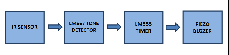
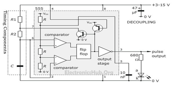
As 555 timer is robust, stable and most commonly used IC in the area of electronics and also use in many electronic circuits. IC 555 is a square wave generator and its duty cycle range from 50% to 100%. The time delay in the circuit is provided by an oscillator. 555 timer IC got its name from the three 5 kilo-ohm resistor attached as a pattern of voltage divider as shown in the below figure. While in the full circuit 555 timer IC consists of many other components via 16 resistors, 20 transistors and 2 diodes also included flip-flop.
Before knowing more about IC first have a glance at the pin diagram.
555 Timer Pin Diagram
Pin Diagram of 555 Timer
Image Source: ElectronicsClub.info/555timer.htm
IC 555 timer is a renowned device in the field of electronics, although the majority of the people does not have any information regarding the internal circuitry as well as about the pins present on the IC.  So here I have tried to explain the working of this IC so that you can build many projects around it and do your experiments.
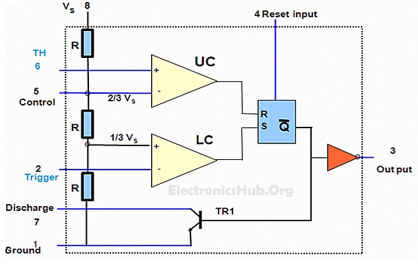
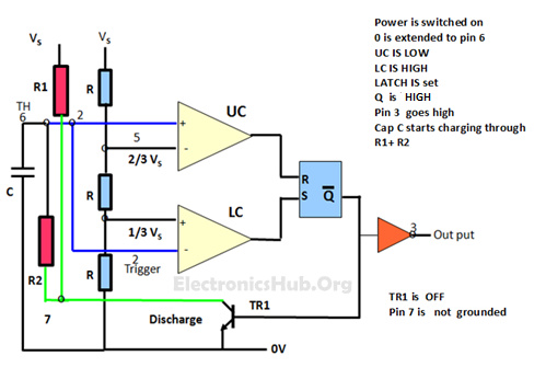
The internal circuitry of the IC in the simplest form is shown below:
Internal Arrangement of 555 Timer
555 Timer – Internal Arrangement
Important Note: The 555 can be used with a supply voltage (Vs) in the range 4.5 to 15V (18V absolute maximum).

Functional Parts of 555 Timer IC:

555 Timer IC has basically three functional parts. They are as follows:
  1. Comparator: It is used to compare two voltages at the input level which is inverting (-) one and non inverting (+). If the voltage at the non-inverting is higher than other than the output is high. For ideal comparator  input resistance is infinite.
  2. Voltage Divider: As the input resistance is infinite in the comparator so the voltage among all three resistors is being divided equally. Value across each resistor is Vin/3.
  3. Flip/Flop: Digital electronic device with memory. If the input is high while low at R then the output at Q is high. It means when S is high Q output is high and if R is high Q output is low.
To get more knowledge about 555 timer, one should need to get aware about the pins. Description of the 555 Timer pins is given below.

Pin Description of 555 Timer:

  1. Trigger Input: If the input <1/3Vs than at that condition output is high. It is useful in examining  the timing capacitor discharging in a stable circuit.
  2. Threshold Input: This pin is attached to the first comparator at the non-inverting input terminal. If the threshold voltage is higher than (2/3) Vin than the output is high at the comparator thus reset the output from high to low in the flip flop.
  3. Reset Input: As based on the internal condition of the flip-flop this pin reset the output of the flip-flop. To get rid  of any noise interference an active low pin is attached to high state till any reset operator is required. So for most of the time it is attached to the supply voltage as in the figure.
  4. Control Input: An external voltage applied to this terminal changes the threshold as well as trigger voltage. Thus by imposing a voltage on this pin or by connecting a pot between this pin and ground, the pulse width of the output wave can be varied. when not used, the control pin should be bypassed to ground with a 0.01uF capacitor to prevent any noise problem.
  5. Discharge Pin: When the timer output is low this pin is connected to 0 volts. It is used to discharge the timing capacitor in astable and monostable mode.
  6. Ground: The reference point or ground point of IC555 is connected to the ground terminal of the dc voltage source, Voltages of the entire circuit are measured with respect to this terminal.
  7. Output: The output of timer and the load is connected to this pin.
  8. Supply: This voltage must be a pure ripple free DC voltage which is obtained by connecting a positive regulated power supply.

Modes of 555 Timer:

The 555 Timer has three operating modes and the details are explained below.
1. Monostable Mode: In this mode, the 555 functions as a “one-shot” pulse generator. Applications comprise many things viz timers, missing pulse detection also included bounce free switches, touch switches as well as frequency divider, capacitance measurement and pulse-width modulation (PWM) and many more.
2. Astable Mode: In this mode, the 555 work as a free running mode. The output of this astable multivibrator toggle between low and high continuously there by generating a train of pulse, that is why it is known as pulse generator.   They are used as an inverter and also used in many of the internal part of the radio. Selecting a thermistor as a timing resistor allows the use of the 555 in a temperature sensor.
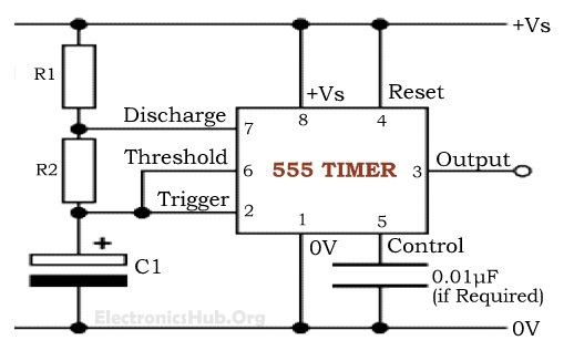
Block diagram of 555 timer in Astable mode is shown below.
Block Diagram of 555 Timer in Astable Mode
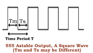
An astable circuit produces a ‘square wave’ and is shown below.
555 Astable Output - A Square Wave3. Bistable Mode or Schmitt Trigger: If there is no capacitor as well as there is no DIS pin used, then 555 timer can work as a flip flop. Its uses Include bounce free latched switches.

555 Timer as Astable Multivibrator:

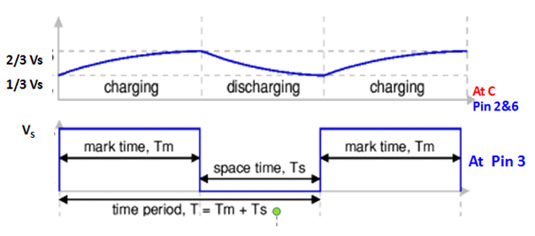
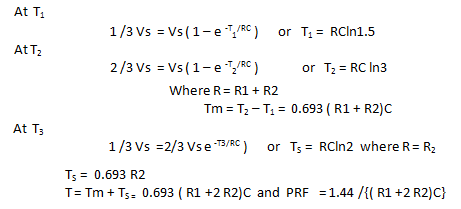
As shown in the diagram below timer 555 works in astable mode along with the internal circuit described in the block. There are three resistors named R inside it and all have equal values. These form a voltage divider having reference voltages of 1/3 and 2/3 of Vcc (the power supply). The logic state of the flip flop is controlled by the reference voltage which is given to one of the inputs of both two comparators.
Pin 2 of the 555 is the trigger input. If the voltage at pin 2 is<1/3 of Vcc, the flip flop switch to a low state of the output of the lower comparator. The output stage has an inverting action. In other words, output at 555 high when flip-flop output is low.
Now imagine if the power supply is first connected to the astable circuit. Timing capacitor is discharged at the starting. The output in 555 is high and voltage is 0V at pin2. With the help of resistor R1 and R2 and capacitor C starts charging. Note that C is also connected to pin 6, which is the threshold input of 555 timer.
555 Timer in Astable Multivibrator Mode - Circuit Diagram
555 Timer in Astable Multivibrator Mode – Circuit Diagram
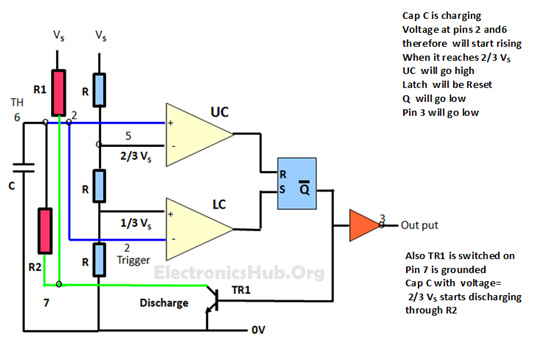
The output of the lower comparator is reached at the next level when the voltage across C is more than 1/3of Vcc. The output of flip flop doesn’t change and remain at low state. The inputs to the second comparator are the voltage at pin 6, the threshold input, and 2/3 VCC from the internal voltage divider. The output of the second comparator reaches for next level when the voltage at C moves more than 2/3 of Vcc. Now the flip flop switch from low to high state and output of 555 also switch from high to low.
Flip-flop is attached with NPN transistor internally and pin 7which is discharge pin of the IC is connected to the collector of the transistor. The transistor gets into On mode when the flip-flop is in high state giving a low resistance path to 0V from the discharging pin. The voltage decreases as the capacitor C starts for vacant via a resistor R2.
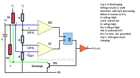
Note capacitor discharges only via R2 while charging via R1 and R2 both. The lower comparator moves to the next level when the voltage across C <1/3 of Vcc, state of flip-flop switches and 555 reaches to high.
The graph below shows how the voltage across the timing capacitor, Vc changes with the output voltage of the 555, Vout.
Voltage Across Timing Capacitor
In short, you can see the above phenomenon in the following pictures.
555 Timer as Astable Multivibrator - Figure 1
555 Timer as Astable Multivibrator – Figure 1
555 Timer as Astable Multivibrator - Figure 2
555 Timer as Astable Multivibrator – Figure 2
555 Timer as Astable Multivibrator - Figure 3
555 Timer as Astable Multivibrator – Figure 3
This cycle repeats continuously.
Above phenomena can be represented below:
555 Timer as Astable Multivibrator - Graphical Representation
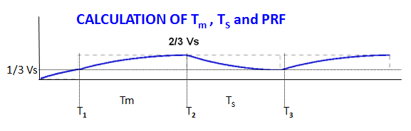
555 Timer as Astable Multivibrator – Graphical Representation
  • Time for which Output is High     = 0.693 (R1+ R2) C
  • Time for which Output is Low Ts = 0.693 R2 C
  • Period of Output T = Tm + Ts       = 0.693(R1+ 2R2)C
  • PRF of Output                                     = 1.44 / (R1+ 2R2)C
  • Duty Cycle Tm/T                              = (R1 + R2)/(R1 + 2R2)‏
Calculation of Tm, Ts and PRFMathematical Calculation of Tm, Ts and PRF
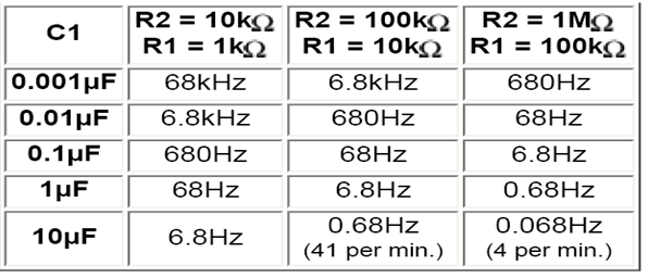
Selection  R1, R2 and C1 for different ferquency range are as follow:
R1 and R2 should be in the range 1k to 1M . It is best to Choose C1 first (because capacitors are available in just a few values)  as per the frequency range  from the following table.
Choose R2 to give the frequency (f) you require.
R2 = 0.7 /(f × C1)‏
Choose R1 to be about a tenth of R2 (1k min.)
Frequency Range Values for 555 Timer in Astable Mode

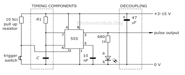
555 Timer IC as Monostable Multivibrator:

Circuit Diagram:
555 Timer as Monostable Multivibrator - Circuit Diagram
555 Timer as Monostable Multivibrator Circuit Diagram – ElectronicsHub.Org
As you can see, the trigger input is kept at HIGH by the 10 kΩ pull up resistor and is pulsed LOW when the trigger switch is pressed. The circuit is triggered by a falling edge, that is, by a sudden transition from HIGH to LOW.
The trigger pulse, produced by pressing the button, must be of shorter duration than the intended output pulse.
The period, t, of the output pulse can be calculated from the design equation:
T=1.1(R*C)

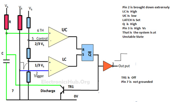
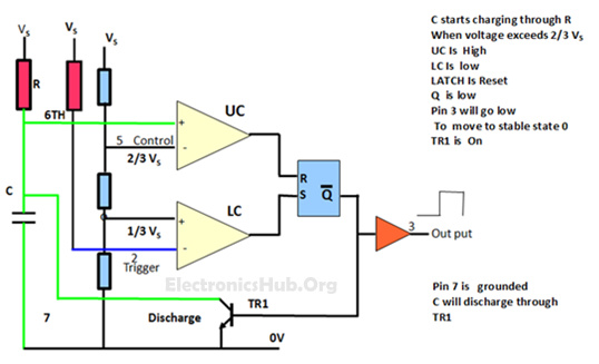
Working of 555 Timer in Monostable mode:


555 timer in Monostable mode - case 1555 timer in Monostable mode – case 1
555 timer in Monostable mode - case 2
555 timer in Monostable mode – case 2
555 timer in Monostable mode - case 3
555 timer in Monostable mode – case 3

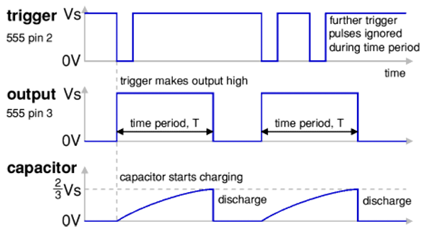
Above phenomenon can be represented as below:
555 timer in Monostable mode - Graphical Presentation
555 timer in Monostable mode – Graphical Presentation
2 /3 Vs  = Vs ( 1 – e -T/RC )               or   T= RC ln3  = 1.1 RC
Brief Description:
  • Monostable  circuit  provides  a single pulse  when   triggered.
  • Monostable  means  one  stable that is  ‘output low’.
  • The ‘output high’  on triggered   is  a temporary  state.
  • The duration of the pulse is called the time period (T) and this is determined by resistor R and capacitor C:
Time period, T = 1.1 × R × C
T = time period in seconds (s)‏
R = resistance in ohms
C = Capacitance in farads (F)‏
Choosing of R and C:
  • Choose C first (there are relatively few values available).
  • Choose R to give the time period required.
  • R should be in the range 1k to 1M.

Posted on Thursday, October 16, 2014 by Unknown

1 comment

This circuit is build around a 555 timer configured in monostable mode means it will be stable in one state and action will require to change that state. That’s why we have utilized this property to make touch on and off switch. With the help of this circuit you do not require to move from your place to on and off the device just touch with the help of finger device will become on and off automatically. And important feature of this circuit is you will not get mechanical shock which we sometimes get while using the normal switched.
Read the related post: How 555 Timer Testing Circuit Works?

Touch ON and OFF Switch Circuit Diagram:

Touch ON and OFF Switch Circuit Diagram
Touch ON and OFF Switch Circuit Diagram by Electronics Hub
Components Used in this Circuit:
  • IC1-NE555
  • R1-3.3M
  • R2-1M
  • On/Off  Switch-Push to on switch
  • Relay-6V, 1 C/0

How Touch ON or OFF Switch Circuit Works?

Assemble the circuit properly and apply power supply. To “ON” the connected device, put your finger between touch to “ON” point and to off the device put your finger between touch to OFF point.
When power supply is provided to circuit device connected through relay remain ideal because voltage at pin2 (trigger pin) of IC is low but as soon as you touch the “ON” switch pin 2 of IC1gets the trigger signals and out pin3 receives high input and output pin 3 goes high which will make the transistor T1 into conduction and the relay connected through it energize and device connected across relay becomes “ON”.
At this point voltage at pin 6 is zero. Similar action takes place when you touch the “OFF” switch. This circuit works by latching a relay to “ON” state with push of a button and with another push latch is released and device become “OFF”. It is working  similar to a flip-flop states.
If you are getting problem in getting touch pad then in place of touch pad you can also switch. In that case use push to on switch so that when you press the switch it will make the connection and “ON” and “OFF” the device according to the requirement.
You can also use the touch plate from the old toys and door bell . Touch pads consist of a small carbon block mounted in silicon rubber and when the button is pushed, the carbon block make contact with the pad and reduces the resistance between the two interleaved tracks. The pads which are available in market  are already protected from corrosion and have very good sensitivity to detect your finger response. When a finger is put between points, the resistance between the lines drops  between 150k and 850k, depending on the pressure and presence of moisture in the finger and it will vary from person to person.

Posted on Thursday, October 16, 2014 by Unknown

No comments